Unlock the Secrets of Microchip Manufacturing
The modern world runs on microchips, tiny components packed with billions of transistors that power everything from smartphones to supercomputers. For decades, the relentless miniaturization of these transistors, following Moore’s Law, has driven technological progress.
However, around 2015, this exponential growth faced significant hurdles. This article digs into the revolutionary technology that not only overcame these limitations but also enabled the creation of the most complex commercial products ever built: Extreme Ultraviolet (EUV) lithography machines.
You will learn about the fundamental process of microchip fabrication, the challenges posed by shrinking transistor sizes, the scientific breakthroughs in X-ray and EUV lithography, and the incredible engineering feats required to create machines capable of printing features with atomic precision. Discover how a single company, ASML, along with its partners, engineered a solution that continues to push the boundaries of what’s possible in semiconductor manufacturing.
Prerequisites
No prior knowledge of semiconductor manufacturing is required, but an interest in advanced engineering and physics will enhance your understanding.
Step-by-Step Guide to Understanding EUV Lithography
Step 1: The Foundation of Microchips – Silicon Wafers
- Silicon Purification: The process begins with silicon dioxide, often sourced from sand. This material is purified into ultra-pure silicon chunks.
- Ingot Formation: The purified silicon is melted in a specialized furnace. A small seed crystal is lowered into the molten silicon. As the seed crystal is slowly raised and rotated, silicon atoms attach to it, forming a large, single-crystal silicon ingot.
- Wafer Slicing and Polishing: The silicon ingot is then precisely cut into thin wafers using diamond wire saws. These wafers are subsequently polished to an extremely smooth finish.
Step 2: Imprinting the Design – Photolithography Basics
- Photoresist Coating: Each wafer is coated with a light-sensitive material called photoresist.
- Mask Exposure: A mask, or reticle, containing the design for a specific chip layer, is used. Light is shone through this mask onto the photoresist. In a positive photoresist, the areas exposed to light become weaker and more soluble.
- Developing the Pattern: The wafer is rinsed with a solution, washing away the weakened, exposed photoresist and leaving the design imprinted on the wafer.
- Etching and Deposition: The exposed silicon underneath the remaining photoresist is then etched away using chemicals or plasma. After etching, a metal, such as copper, is deposited to fill the etched lines.
- Cleaning: The remaining photoresist is washed away, completing one layer of the chip.
- Layer Repetition: This cycle of coating, exposing, etching, and depositing repeats for every layer of the chip, which can range from 10 to over 100 layers. The bottom layers typically form the transistors, while higher layers form the intricate wiring.
Step 3: The Challenge of Miniaturization
The critical step determining how small features can be made is photolithography. As feature sizes shrink, they approach the wavelength of the light used, leading to diffraction and interference problems. These phenomena cause the light waves to bend and overlap, making it difficult to print sharp, precise patterns.
- Diffraction: Light passing through small gaps in the mask diffracts, spreading out. When waves from different gaps overlap, they can cancel each other out (destructive interference) or reinforce each other (constructive interference), distorting the intended pattern.
- Working with Diffraction: Chip designers have learned to use diffraction by carefully designing the mask patterns so that the resulting interference creates the desired layout on the wafer.
- Numerical Aperture (NA): The ability of a lens system to capture light and resolve fine details is described by its Numerical Aperture (NA). A higher NA allows for the printing of smaller features.
- Wavelength Limitation: The Rayleigh Equation relates the smallest feature size (critical dimension) to the wavelength of light and the NA. To print smaller features, either NA must increase, or the wavelength must decrease.
- The Limit of Deep UV: For decades, the industry used deep ultraviolet (DUV) light with a wavelength of 193 nanometers. By the mid-2010s, further reductions in feature size using DUV reached fundamental physical limits, stalling Moore’s Law.
Step 4: The Quest for Shorter Wavelengths – X-rays and EUV
To overcome the limitations of DUV, scientists explored much shorter wavelengths, like X-rays (around 10 nanometers). However, X-rays are readily absorbed by air and most materials, making them difficult to work with. They also require specialized mirrors instead of conventional lenses for focusing.
- X-ray Lithography: Early research by scientists like Hiroo Kinoshita proposed using X-rays, but practical challenges included generating the X-ray source and developing reflective optics.
- Multilayer Mirrors: A breakthrough came with the development of multilayer mirrors, consisting of alternating thin layers of materials like tungsten and carbon. These mirrors could reflect X-rays at specific angles.
- The Mirror Challenge: Reflecting X-rays required mirrors of unprecedented smoothness. If scaled to the size of the Earth, the largest bump on these mirrors could only be as thick as a playing card.
- Extreme Ultraviolet (EUV): The concept evolved towards Extreme Ultraviolet (EUV) light, with wavelengths around 13.5 nanometers. EUV is less energetic than X-rays but still requires a vacuum environment and specialized reflective optics.
Step 5: Engineering the Impossible Machine – ASML’s EUV Lithography System
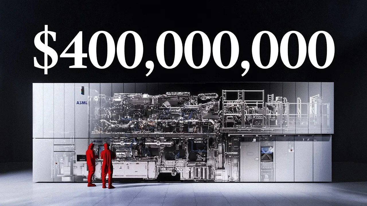
Developing a practical EUV lithography machine presented immense engineering challenges. The machine is one of the most complex commercial products ever created, costing hundreds of millions of dollars.
- The Core Process: The machine uses a powerful laser to hit tiny droplets of molten tin, creating a plasma that emits EUV light. This light is then precisely directed by a series of ultra-smooth multilayer mirrors onto the wafer’s mask (reticle) and then onto the wafer itself.
- Precision and Speed: The system must perform incredibly demanding tasks with atomic-level precision and at high speeds:
- Laser Precision: It fires a laser three times in 20 microseconds to hit a single droplet of tin, heating it to over 220,000 Kelvin.
- Droplet Control: It generates and precisely targets 50,000 tin droplets every second.
- Mirror Quality: The mirrors used are among the smoothest objects in the universe; if scaled to Earth’s size, their largest imperfections would be no thicker than a playing card.
- Alignment Accuracy: It overlays chip layers with an accuracy no greater than five atoms.
- Acceleration: Parts of the machine move at accelerations exceeding 20 Gs.
- The Light Source: Generating the necessary EUV light is a major hurdle. The system uses a laser-produced plasma (LPP) method. A high-power laser strikes microscopic droplets of tin.
- Tin Droplet Technology: To achieve the required efficiency and wavelength (around 13.5 nm), tin is used. The challenge is to create perfectly uniform droplets at a rate of 50,000 per second. ASML perfected a method to modulate a tin jet, causing it to break into highly uniform droplets that are then precisely hit by the laser.
- Mirror System: The EUV light is reflected by multiple (typically six) ultra-smooth multilayer mirrors before reaching the reticle and then projected onto the wafer. Each mirror has a reflectivity of about 70%, but even with multiple reflections, significant light loss occurs.
- Overcoming Light Loss: To compensate for light loss through the mirror system, the EUV light source must be extremely powerful (over 100 watts). The tin droplet LPP method, with its high conversion efficiency, is key to achieving this power output.
- The Role of ASML: ASML, a Dutch company, became the sole manufacturer capable of producing these complex EUV machines, collaborating with partners like Zeiss for the optics. Their engineering prowess and persistence, building on decades of research from labs and universities worldwide, made EUV lithography a commercial reality, saving Moore’s Law.
Step 6: The Impact of EUV Lithography
EUV lithography allows for the printing of significantly smaller and more complex features on microchips than was previously possible. This enables the production of more powerful, energy-efficient, and smaller electronic devices, continuing the advancement of technology in the nano-scale era.
Source: The World's Most Important Machine (YouTube)