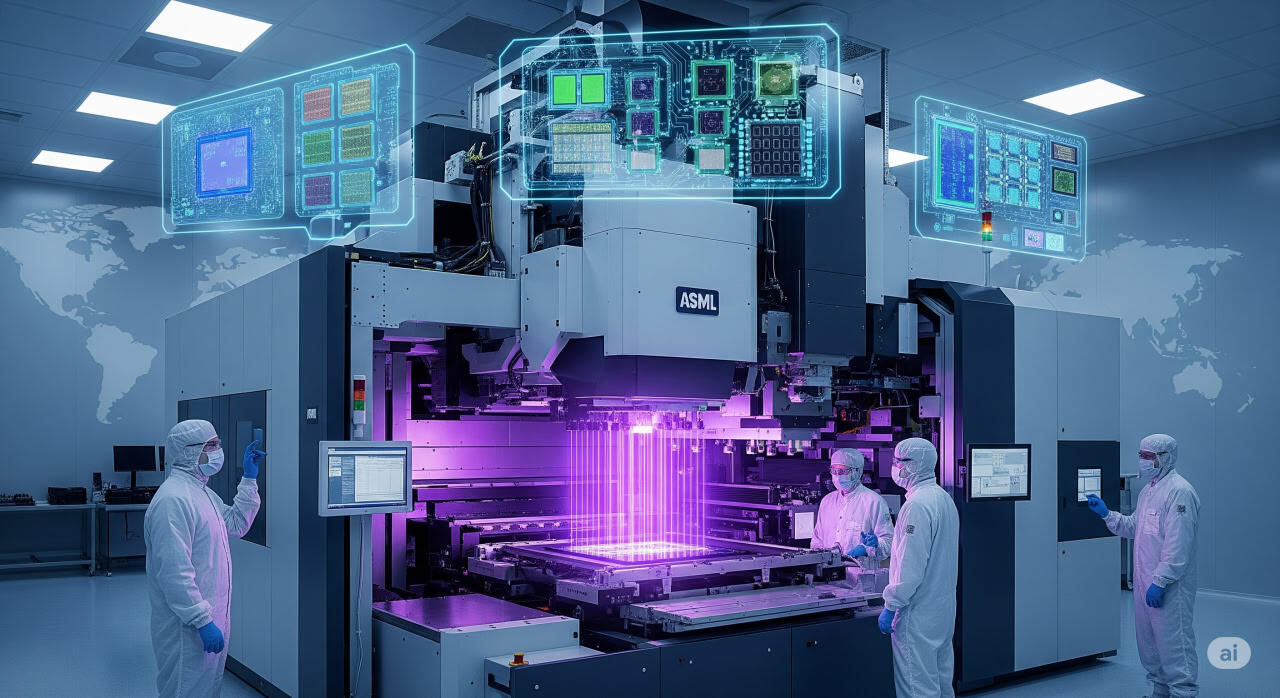
In the heart of the Netherlands, amid sprawling cleanrooms and humming assembly lines, lies a technological marvel that’s reshaping the semiconductor industry: ASML’s High NA EUV lithography machine. Priced at a staggering $400 million and larger than a double-decker bus, this behemoth is the pinnacle of human engineering, capable of etching circuits finer than ever before onto silicon wafers.
As demand for advanced chips skyrockets with the AI boom, ASML’s latest innovation isn’t just a tool—it’s a gateway to smaller, faster, and more efficient processors that power everything from smartphones to supercomputers. But with geopolitical tensions, including U.S. Tariffs and export controls, casting shadows over global supply chains, the road ahead for this Dutch giant is as complex as the machines it builds.
The Genesis of ASML: From Humble Beginnings to Lithography Dominance
ASML’s story is one of audacious bets and relentless innovation, rooted in the fertile tech ecosystem of Eindhoven, Netherlands. Founded in 1984 as a spin-off from Philips Electronics, the company started in a modest leaky shed, focusing on lithography—the art of projecting intricate patterns onto silicon wafers to create microchips. Lithography is the backbone of semiconductor manufacturing, determining how small and dense transistors can be, directly influencing chip performance and power efficiency.
In its early days, ASML competed in a crowded field with Japanese giants like Nikon and Canon, producing deep ultraviolet (DUV) lithography machines that used 193-nanometer wavelengths of light. These tools were sufficient for the chips of the 1990s and early 2000s, but as Moore’s Law—the prediction that transistor counts double every two years—pushed boundaries, the industry needed something revolutionary. Transistors shrank to nanoscale sizes, demanding wavelengths short enough to etch features just a few atoms wide.
Enter extreme ultraviolet (EUV) lithography, a concept ASML pursued aggressively starting in the late 1990s. EUV uses light at a 13.5-nanometer wavelength—about 14 times shorter than DUV—allowing for unprecedented precision. However, generating and controlling EUV light was a Herculean task.
It required creating a vacuum environment, as EUV is absorbed by air, and developing mirrors flatter than any surface ever made to reflect this elusive light. ASML invested billions, filing hundreds of patents annually, and by 2018, it had cornered the EUV market entirely. No other company has successfully commercialized EUV, giving ASML a monopoly on the technology essential for the most advanced chips from Nvidia, Apple, Intel, TSMC, and Samsung.
Today, ASML employs over 44,000 people worldwide, with 8,500 in the U.S. Alone, and operates 60 global offices. Its revenue trajectory reflects the chip industry’s explosive growth: In Q2 2025, ASML reported €7.7 billion in net sales and €2.3 billion in net income, projecting a 15% revenue increase for the full year to between €30 billion and €35 billion, with a gross margin around 52%.
EUV systems, though only 8% of units sold in 2024 (44 out of 418 machines), accounted for 38% of system sales revenue due to their high price tags of up to $220 million each. This dominance has propelled ASML’s market capitalization to over €350 billion, making it Europe’s most valuable tech company.
Yet, ASML’s success isn’t without peril. The company’s reliance on a global supply chain—sourcing mirrors from Germany’s Zeiss, lasers from the U.S., and components from hundreds of suppliers—exposes it to disruptions. Geopolitical factors, such as U.S. Export controls barring EUV sales to China since 2019, have shifted dynamics.
China once accounted for up to 49% of ASML’s business through DUV sales, but by late 2024, that dropped to 30% as backlogs cleared and restrictions tightened. Amidst this, ASML’s pivot to High NA represents not just technological advancement but a strategic necessity to stay ahead in an increasingly fractured world.
Demystifying EUV: The Science Behind the Magic
To appreciate High NA, one must first understand EUV lithography, the foundation upon which it’s built. Chips are fabricated on silicon wafers—thin, circular slices about 300mm in diameter—layer by layer, up to 100 times, forming billions of transistors. Each layer is patterned using lithography: light projects a blueprint (mask) onto a photosensitive chemical (photoresist) coating the wafer.
Traditional DUV uses 193nm light, but as transistors shrank below 7nm, diffraction limits blurred patterns. EUV’s 13.5nm wavelength solves this, enabling features as small as 5nm or less. However, producing EUV light is extraordinarily complex.
ASML’s system fires 50,000 molten tin droplets per second, vaporizing them with a CO2 laser hotter than the sun’s surface to create plasma that emits EUV photons. This plasma is captured by a collector mirror from Zeiss, then bounced through a series of ultra-flat mirrors (deviations less than 1/10th of a nanometer) in a vacuum chamber to prevent absorption.
The light passes through the projection optics, hitting the wafer at nanosecond precision. TSMC likens the accuracy to hitting a coin on Earth with a laser from the Moon.
The wafer stage moves at speeds up to 200mm/s, aligning with sub-nanometer accuracy. Each EUV machine processes about 200 wafers per hour, aiming for hundreds more, producing millions annually.
Power consumption is a hurdle: EUV systems guzzle energy, but ASML has reduced wafer exposure energy by over 60% since 2018. Still, unchecked AI training could consume global energy by 2035, highlighting the need for efficiency. DUV remains vital for less advanced layers, comprising over half of ASML’s revenue, with machines priced from $5 million to $90 million.
EUV’s development spanned 20 years and billions in R&D, nearly bankrupting ASML. Key customers like Intel, TSMC, and Samsung invested heavily—Intel alone poured $4 billion in 2012—to keep it afloat. This collaboration highlights the symbiotic relationship: Without EUV, advanced AI chips like Nvidia’s H100 wouldn’t exist.
The High NA Breakthrough: Pushing the Boundaries of Precision
High NA EUV, developed since 2016, builds on this foundation with a critical enhancement: a larger numerical aperture (NA). NA measures the lens’s light-gathering angle; standard EUV is 0.33, High NA jumps to 0.55, capturing steeper light rays for sharper resolution. This allows single-exposure printing of sub-3nm features, versus multiple exposures (and masks) in standard EUV, reducing complexity, cycle time by up to 60%, and boosting yield.
The trade-off? Size and cost. High NA requires larger mirrors, making the machine enormous—shipped in parts via seven Boeing 747s and 25-30 trucks.
Assembly takes 18 months, involving 100,000 parts and 40,000 bolts. Intel received the first in Oregon last year, producing 30,000 wafers with doubled reliability. TSMC is evaluating for future nodes, while Samsung reports efficiency gains.
Shipments are ramping: Five in 2024, aiming for 20 annually soon. High NA sales tripled projections, from €465 million in 2024 to €1.7 billion in 2025, driving EUV’s overall surge. This aligns with AI demand: Without High NA, scaling AI models becomes cost-prohibitive.
Analysis: High NA exemplifies Moore’s Law’s persistence, but at escalating costs. Fabs must weigh $400 million per machine against productivity gains. For Intel, it’s a lifeline to catch TSMC; for others, a step toward 2nm and beyond.
Geopolitical Headwinds: Tariffs, Export Controls, and Supply Chain Risks
ASML’s global footprint—80% of sales in Asia—exposes it to U.S.-China tensions. Since 2019, U.S. Controls ban EUV/High NA sales to China, fearing military use.
China stockpiled DUV, but advanced nodes lag. Huawei’s 7nm chips rely on multi-patterning, inefficient for scale.
Trump’s 2025 tariffs add uncertainty: 10-50% on EU goods, though semiconductors may be exempt or low. ASML’s shares dropped 10.5% post-Q2 earnings amid tariff fears, with 2026 growth unassured. CEO Fouquet notes potential impacts but emphasizes advocacy for minimal duties.
U.S. CHIPS Act ($52B subsidies) boosts domestic fabs, prompting ASML’s Arizona training center for 1,200 annually. Intel’s Ohio/Arizona fabs and TSMC’s Phoenix plant signal onshoring, reducing Asia reliance.
China’s response: Investing in domestic lithography, but experts doubt quick EUV replication. Tariffs could spark retaliation, disrupting ASML’s suppliers.
Implications: Tariffs may accelerate U.S. Independence but raise costs, slowing AI innovation. ASML’s monopoly provides leverage, but over-reliance risks backlash.
Beyond High NA: Hyper NA and the Horizon of Chip Innovation
ASML isn’t resting: Hyper NA, with NA >0.7, targets sub-1nm features, debuting 2030-2035. It promises further shrinks, but challenges abound—larger optics, higher power, and costs potentially $700 million. Fouquet stresses customer need; without it, adoption lags.
Future lithography may integrate AI for optimization, or explore alternatives like nanoimprint. But EUV’s roadmap extends Moore’s Law to 2035+.
Analysis: Hyper NA could enable exascale computing, revolutionizing AI/drug discovery. Yet, physical limits loom—quantum effects at atomic scales demand new paradigms like 3D stacking or neuromorphic chips.
The Broader Impact: Powering AI While Navigating Ethical and Environmental Challenges
High NA’s arrival coincides with AI’s insatiable hunger for compute. Nvidia’s Blackwell chips, made with EUV, deliver 30x AI inference gains. But energy demands are colossal; data centers could consume 8% of U.S. Power by 2030.
Ethically, ASML’s tech enables surveillance/AI weapons, raising dual-use concerns. Environmentally, fabs guzzle water/power, prompting sustainability pushes.
In conclusion, ASML’s High NA machine isn’t just engineering triumph—it’s the linchpin of digital future. Amid tariffs and rivalries, its success hinges on collaboration. As chips shrink, possibilities expand, but so do responsibilities.